AustinIO > Giga Austin Nexus > Terafab Research Fab
Terafab Research Fab at Giga Texas
The Fab Leg of the Texas Industrial Triad
The Terafab Research Fab is the fab leg of the Texas Industrial Triad anchored at Giga Austin, one of the three foundational machine types (gigafactory, fab, datacenter) that run the new industrial-AI economy. See Texas Industrial Triad for the full anchor-facility framework.
Elon Musk unveiled the Terafab joint venture between Tesla, SpaceX, and xAI on March 21, 2026, framing it as a vertically integrated semiconductor complex covering chip design, lithography, fabrication, memory production, advanced packaging, and testing under a single roof. Intel joined as foundry partner on April 7, 2026. Tesla broke ground on the North Campus of Giga Texas on April 22, 2026, committing $3 billion as initial capital. Tesla's Q1 2026 Form 8-K identifies the Research Fab as the first concrete deliverable of the broader Terafab program and discloses that the final chip design of the next-generation AI5 inference processor was completed in April 2026, the silicon the Research Fab is being built to iterate on.
That $3 billion is the most-cited number in coverage and the most misunderstood. It is Tesla's initial cash commitment, not the equipped cost of the facility. A leading-edge 2nm-class research fab realistically costs $25-30 billion fully tooled. Tesla's $3 billion is plausibly the lithography stack alone, three to five EUV scanners at $200-350 million each before any metrology, deposition, etch, CMP, ion implantation, inspection, or facilities cost. The capital gap between Tesla's contribution and the facility's full equipped cost is the practical reason Intel's role on the Research Fab is structural, not optional.
Two-Facility Architecture
The Research Fab and the future production fab are different buildings, at different locations, with different scales, and different roles in Tesla's silicon strategy.
| Dimension | Research Fab | Production Fab |
|---|---|---|
| Location | Giga Austin North Campus | Gibbons Creek Reservoir, Grimes County |
| Output Scale | A few thousand wafer starts per month | 100K-1M wafer starts per month at full scale |
| Primary Role | Rapid iteration of process recipes, transistor architectures, packaging variants | Volume manufacturing of validated designs |
| Status | Groundbreaking April 22, 2026 | Grimes County public hearing June 3, 2026 |
Intel brings the process technology, equipment expertise, packaging capability, and manufacturing scale; Tesla, SpaceX, and xAI bring the demand base, chip design work, and capital. This page covers the Research Fab; the production fab at SpaceX Reinvestment Zone No. 1 - 2026-001, approximately 20 miles east of Bryan-College Station, is covered separately at Terafab Production Facility (Grimes County).
Why a Research Fab
A new process recipe at sub-2-nanometer nodes requires multiple weeks of wafer time per iteration, a full set of EUV lithography and metrology tools, and a production-scale fab line to validate. At a high-volume foundry, the line cannot be taken out of revenue production to run experimental recipes. New process nodes are therefore historically developed at dedicated R&D fabs.
| Operator | R&D Fab | Location |
|---|---|---|
| TSMC | Fab 12 | Hsinchu, Taiwan |
| Intel | D1X | Hillsboro, Oregon |
| Samsung | S1 | Giheung, South Korea |
| Tesla / Intel | Terafab Research Fab | Giga Austin North Campus |
The few-thousand-wafer-per-month scale is sized for experiments, not commerce: enough volume to qualify a new recipe and characterize yield, not enough to materially serve any of Tesla's chip programs at the scale Cybercab, Optimus, and Starlink require. Volume production goes to the production fab. The two facilities are complements, not redundancies.
Intel's Role at the Research Fab
Intel's role almost certainly extends to the Research Fab itself, not just the eventual production fab. The reasons are operational, not contractual, and reduce to two binding constraints Tesla cannot solve on its own at the timeline the construction pace implies.
WFE supply chain. ASML, the sole producer of EUV lithography systems globally, does not sell to new-entrant fab customers without a multi-year technical readiness review and relationship development period. TSMC, Samsung, and Intel each went through that process over years before receiving their first EUV systems. A Research Fab targeting first wafer output on a 2026-2027 timeline cannot wait. Intel's existing ASML position, with multiple EUV systems installed at Arizona and Oregon and an established High-NA EUV queue position, provides the only path by which Tesla can secure scanners on the announced timeline. The same logic applies across Applied Materials, Lam Research, Tokyo Electron, and KLA, each operating multi-year queues with allocation priority for incumbent operators.
Operational expertise. Process integration engineering, yield ramp methodology, contamination control, statistical process control, and tool qualification protocols are capabilities developed over decades, not skills hired in over months. Intel has them; Tesla does not at leading-edge nodes. The Research Fab will need Intel engineers on the floor, Intel process recipes as starting points for Tesla's experimental variants, and Intel-led tool installation and qualification.
Intel's April 7 statement described its contribution as "design, fabricate, and package ultra-high-performance chips at scale," language that describes the entire fab function. The trade is implicit: Tesla retains the Research Fab as the site where chip-and-fab co-design experiments tailored to AI6, AI7, and successor silicon happen; Intel provides the operational substrate that makes those experiments executable. For the three-tier fab strategy that Terafab completes (Samsung Taylor as captive-equivalent for AI5, TSMC Arizona as supply-resilience second source, Terafab as owned production for AI6 and AI7), see SemiconductorX: Tesla Terafab Supply Chain.
What the Research Fab Iterates On
Tesla's Q1 2026 8-K disclosure that the final chip design of AI5 was completed in April 2026 anchors the near-term focus. AI5 is moving from design to production at Samsung Taylor and TSMC Arizona simultaneously, while the Research Fab in Austin iterates on AI6 and AI7.
| Chip | Application | Optimization Priority | Manufacturing Path |
|---|---|---|---|
| AI5 | Vehicle inference (HW5) | Maximum TOPS at datacenter-class TDP | Samsung Taylor (captive) + TSMC Arizona (resilience) |
| AI6 | Cybercab and Optimus low-power inference | Maximum efficiency per watt within compact thermal budget | Research Fab iteration to production fab volume |
| AI7 | SpaceX orbital compute (Starlink and successors) | Radiation-tolerant continuous AI in LEO | Research Fab process modifications to production fab |
AI6 inverts the AI5 tradeoff, prioritizing maximum inference efficiency per watt within a thermal budget compatible with compact robotaxi and humanoid form factors. AI7 requires process modifications no commercial foundry will develop for a single customer: hardened cell libraries, error-correcting code on all memory, triple modular redundancy on safety-critical control paths, deep n-well guard rings, and TID-tolerant process parameters. The Grimes County production fab filing's reference to Intel 14A process technology (per Musk's Q1 2026 earnings call) suggests AI7's radiation-tolerant variants may co-develop with the 14A node ramp at Grimes County rather than the Research Fab's Intel 18A line, with the Research Fab's role becoming process-recipe transfer and qualification rather than primary AI7 development.
The chip-and-fab co-design loop is structurally what makes AI6 and AI7 possible. Each chip is co-designed with the process variant it will run on, with optimization decisions made simultaneously in the silicon and in the lithography rather than the chip designer accepting a fixed PDK from an external foundry. Validated recipes transition to volume production at the Intel-operated production fab once the Research Fab has characterized yield.
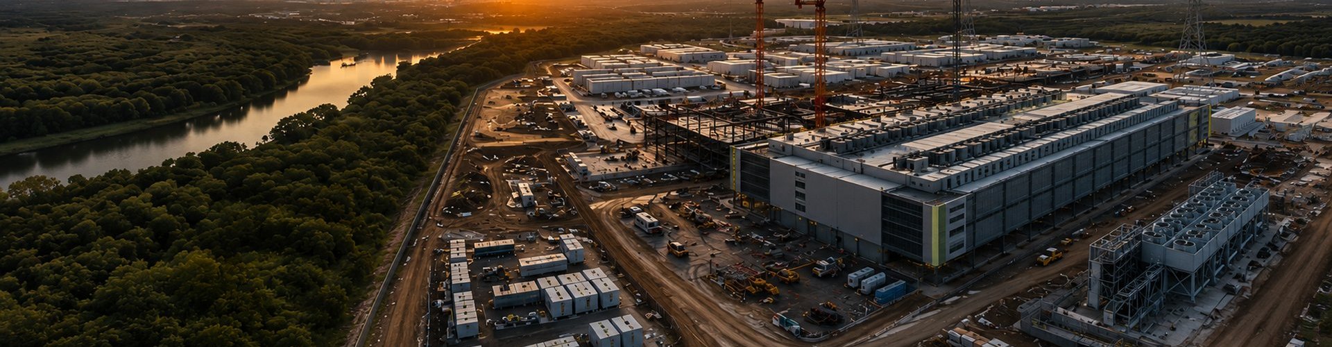
Construction Status
Verified drone observation by Joe Tegtmeyer documented active earthwork and foundation preparation by April 13, 2026, focused on three priorities: extending River Road, installing water retention and drainage systems, and relocating existing workshops and trailers to clear the construction footprint. The compressed timeline (March 21 announcement, April 7 Intel partnership, April 22 groundbreaking) is itself analytically significant. Standard semiconductor fab construction proceeds on multi-year planning cycles before visible site work; Terafab moved from announcement to active earthwork in under five weeks. Significant site preparation, permit coordination, and partnership negotiation must have proceeded in parallel with the public announcement timeline rather than after it.
Capital Reality and the $5 Trillion Number
The capital figures associated with Terafab span four orders of magnitude depending on what is being measured. Conflating them is the most common analytical error in Terafab coverage.
| Figure | Source | What It Represents |
|---|---|---|
| $3 billion | Musk, April 22, 2026 | Tesla initial cash commitment to begin Research Fab construction |
| $25-30 billion | Industry comparable (TSMC, Intel, Samsung) | Realistic equipped cost of Research Fab at 2nm-class capability |
| $20-25 billion | Musk, March 21, 2026 | Stated initial range for broader Terafab project (likely understated) |
| $35-45 billion | Morgan Stanley | Estimate for "meaningful chipmaking capacity" |
| $55-119 billion | SpaceX filing | Initial production fab capital ($55B) and full buildout ($119B) |
| ~$5 trillion | Bernstein, March 26, 2026 | Full vertically integrated buildout at announced 1 TW/year compute scale |
Tesla's $3 billion likely covers the EUV lithography stack and a portion of facilities cost. The remainder of the equipped fab cost is borne by the broader joint venture with Intel as the operational and capital partner that closes the gap. Capital equipment alone runs $8-12 billion at this scale (15-20 EUV systems plus the full process tool set).
The May 6, 2026 Grimes County tax abatement filing, by SpaceX rather than Tesla, provided the first concrete capital figure for the production fab itself. The $55 billion initial-phase commitment substantially exceeds Morgan Stanley's $35-45 billion meaningful-capacity estimate. The split filing entity clarifies the operational division Musk confirmed during Tesla's Q1 2026 earnings call: SpaceX handles high-volume chip manufacturing at the production fab, while Tesla operates the smaller R&D pilot line at Giga Austin's Research Fab.
Bernstein's $5 trillion is not a prediction. It is Bernstein's estimate of what fulfilling Terafab's announced 1-terawatt-per-year compute target would actually require. The math: full buildout across logic fabs alone runs approximately $3.15 trillion at 100 percent yield or $3.78 trillion at the 80 percent yield realistic for a new-entrant operator, with memory production and advanced packaging adding more. The semiconductor industry's collective annual capex globally runs $200-250 billion. Bernstein's $5 trillion implies a capital program 20-25 times that annual rate, sustained over years. The Research Fab on the North Campus, at $25-30 billion equipped cost, is the only element of the program with a credible near-term execution path.
Substrate Dependency and Campus Integration
The Research Fab requires ultra-pure water at semiconductor-grade specifications, EUV-class power stability, vibration isolation from the adjacent vehicle factory operations, and a workforce density of process and yield engineers that the Austin metro semiconductor cluster (documented at Austin Semiconductor Ecosystem) is uniquely positioned to supply.
The integration extends from chip to humanoid to compute to OTA. AI6 silicon iterating at the Research Fab feeds Optimus humanoid units being manufactured at the adjacent Optimus factory. Those units generate operational data that feeds the Cortex 2 training cluster on the same campus. The trained models push back via OTA. The same recursive integration that defines the EV production line, chips designed at the campus, made at fabs Tesla controls or co-anchors, deployed in vehicles and humanoids built at the campus, training data flowing back to the campus's compute clusters, extends to the Research Fab as the closest physical instantiation of chip-and-fab co-design Tesla operates. The Research Fab is the smallest of the four programs by output volume and the most capital-intensive per square foot, but it is the program that ties the campus's silicon strategy to the silicon physically.
Research Fab Snapshot (Q2 2026)
| Dimension | Detail |
|---|---|
| Location | North Campus, Giga Texas, Austin |
| Operational Model | Tesla-led with Intel as foundry partner; Intel role spans WFE procurement, process expertise transfer, tool qualification, and operational support |
| Tesla Initial Capital Commitment | $3 billion (announced April 22, 2026; covers lithography stack and partial facilities) |
| Realistic Equipped Cost | $25-30 billion fully tooled (industry comparable for 2nm-class research fab) |
| Output Scale | A few thousand wafer starts per month (experimental scale) |
| Primary Function | Rapid iteration of process recipes, transistor architectures, packaging variants for AI5 successors, AI6, and AI7 |
| JV Partners | Tesla, SpaceX, xAI; Intel as foundry partner (announced April 7, 2026) |
| Process Node | Intel 18A (1.8nm-class, gate-all-around, backside power delivery via PowerVia, EMIB and Foveros packaging); roadmap toward Intel 14A |
| Groundbreaking | April 22, 2026 (announced March 21, 2026; Intel partnership April 7, 2026) |
Outlook
The Research Fab's 2026-2027 trajectory is the most credible near-term execution path within the broader Terafab program, credible specifically because Intel is the operational partner. Developing a 2nm process from first principles as a new-entrant fab operator at multi-trillion-dollar scale would have required 5-7 years of yield learning and capital availability beyond what any private joint venture has ever assembled. The April 7 Intel partnership reframed the program's risk profile materially: the Research Fab inherits a process Intel has already qualified at high-volume manufacturing scale (Intel 18A at Arizona and Oregon), established WFE procurement relationships, and the operational expertise to qualify tools and ramp yield on a leading-edge process.
Near-term operational questions resolving in 2026-2027: whether the Research Fab reaches first wafer output on the timeline the construction pace suggests; whether the AI6 and AI7 process iterations validate at the scale needed to transition to the production fab; whether Intel's 18A process accommodates the radiation-tolerant variants AI7 requires for SpaceX orbital deployment; whether the chip-and-fab co-design loop produces the performance advantages Tesla's silicon thesis depends on. Longer-term capital questions resolve over the back half of the decade: whether the Grimes County production fab's $55 billion initial-phase commitment converts to operational capacity on a credible timeline, and whether the $119 billion full-buildout figure is achievable.
The May 6, 2026 Grimes County filing materially shifts the program's risk profile. The production fab moves from "TBD" to a brownfield site (former Texas Municipal Power Agency coal-fired plant, 1982-2018) with existing power infrastructure, water access (Gibbons Creek Reservoir), and transmission capacity inherited from the prior coal generation. The site selection plus the $55-119 billion capital framework substantially de-risks the production fab side; the Research Fab on the North Campus remains the chip-and-fab co-design substrate that the production fab cannot replace. The Research Fab is the smallest, fastest, and most realistic element of the Terafab program, and the only element currently visible on the Giga Austin North Campus.
Related Coverage
Giga Austin Nexus | Electric Vehicle Production | Optimus Humanoid Production | Cortex AI Compute | Terafab Production Facility (Grimes County) | Texas Industrial Triad | SemiconductorX: Tesla Terafab Supply Chain | Texas Energy Nexus | UT Austin Nexus | Austin Strategic Capital Nexus | Austin Semiconductor Ecosystem