AustinIO > Texas Nexus > Brazos Valley Semiconductor Concentration > Texas A&M Semiconductor Institute / RELLIS
Texas A&M Semiconductor Institute / RELLIS
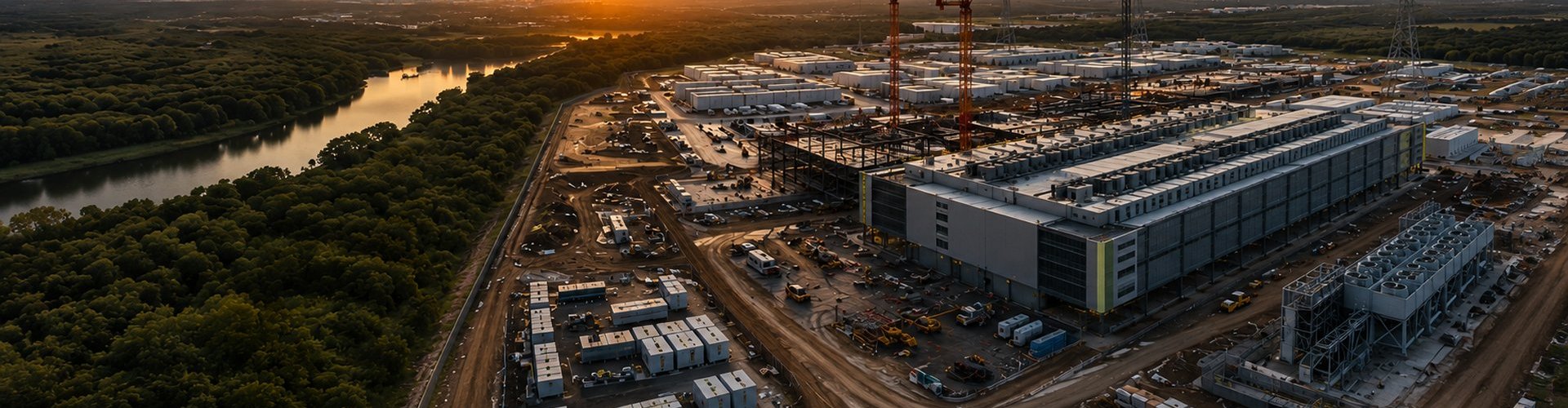
The Texas A&M Semiconductor Institute (TSI) is the $226.4 million Texas CHIPS Act-funded semiconductor research and development substrate at Texas A&M System's RELLIS Campus near Bryan. Designed by Stantec, the 80,000 square foot two-story facility broke ground April 9, 2026, in a ceremony attended by Governor Greg Abbott, TAMU System Chancellor Glenn Hegar, A&M System Regent Jay Graham, A&M System Vice Chancellor for Research Dr. Joe Elabd, plus the institute's inaugural director Dr. Steve E. Putna. Construction is targeted for completion by the first quarter of 2028. The facility features Class 100 and Class 1000 cleanrooms with leading-edge 300mm equipment, ballroom-style reconfigurable layout, plus specialized labs for lithography, metrology, packaging, radio frequency, photonics, process and tooling development, and testing and evaluation. The Texas A&M Board of Regents allocated an additional $205.5 million in school funds for the capital improvement project plus related equipment, making TSI the most expensive undertaking per square foot in the university's history.
TSI represents the academic-and-workforce-development anchor of the Brazos Valley Semiconductor Concentration, complementing the prospective commercial semiconductor manufacturing operators (Substrate Inc.'s Project Factory One on the same RELLIS Campus, the Terafab Production Facility at Gibbons Creek in Grimes County) plus the broader Texas A&M System research substrate (Center for Microdevices and Systems via AggieFab Nanofabrication, Cyclotron Institute, broader engineering research substrate). The facility's strategic position combines federally-coordinated semiconductor research with industry partnership integration (existing TAMU System partnerships with Samsung, Tokyo Electron America, Cadence, plus the memorandum of understanding with Substrate Inc.) plus workforce development pipeline scaling. Combined with UT Austin's Texas Institute for Electronics (TIE, the $440 million Texas CHIPS Act-funded sister substrate at the Austin metro), TSI anchors the federally-coordinated Texas academic semiconductor research substrate at state scale.
Site and Substrate
The TSI facility occupies undeveloped land at Texas A&M System's RELLIS Campus, the 3,300-acre research and innovation hub located approximately eight miles from the Texas A&M University main campus in College Station. The TSI building is positioned behind the RELLIS Research Integration Center (RIC), establishing the facility as the semiconductor-specific research anchor within the broader RELLIS substrate. RELLIS represents Texas A&M's $1.5 billion investment in research and innovation infrastructure anchored by transportation innovation, national security and defense, energy production and reliability, artificial intelligence hypercomputing, plus the emerging semiconductor research substrate that TSI consolidates.
The site selection logic reflects multiple structural factors. RELLIS Campus's existing semiconductor and microelectronics research substrate (AggieFab Nanofabrication facility, Cyclotron Institute, Center for Microdevices and Systems, broader engineering research operations) supports operator-academic integration. Texas A&M System's existing partnerships with semiconductor industry operators (Samsung at Taylor in Williamson County, Tokyo Electron America's broader US substrate, Cadence's EDA software substrate, plus the memorandum of understanding with Substrate Inc. for Project Factory One on the same RELLIS Campus) supports operator coordination at scale. The Brazos Valley regional substrate (covered at Brazos Valley Semiconductor Concentration) provides workforce, supplier ring, water rights, transmission infrastructure, plus integration with the broader Texas Triangle. The 80,000 square foot footprint plus the building's ballroom-style reconfigurable cleanroom layout reflects design priorities for adaptable research substrate that supports evolving semiconductor research priorities across the multi-decade operational lifetime.
Capital Reality
TSI's capital framework operates across multiple coordinated tiers. The $226.4 million Texas CHIPS Act allocation under HB 5174 (2023) breaks down as approximately $200 million for the TSI building plus $26.4 million for the Center for Microdevices and Systems (operating mainly through the school's AggieFab Nanofabrication facility per Associate Dean of Engineering Research Arum Han, Ph.D.). The Texas A&M Board of Regents Feb. 5, 2026 agenda allocated an additional $205.5 million in school funds for the capital improvement project plus related equipment. Combined committed TSI substrate capital substantially exceeds $431.9 million across the Texas CHIPS Act allocation plus TAMU System Board allocation; the institute represents the most expensive undertaking per square foot in the university's history per multiple sources including TAMU System officials. Approximately $161.8 million of the Board allocation is designated specifically for building construction.
Process Technology and Research Focus
TSI's process technology and research focus reflects the facility's positioning as research-and-development substrate rather than volume manufacturing. The Class 100 and Class 1000 cleanrooms accommodate semiconductor research at production-like cleanliness specifications without the volume manufacturing throughput requirements of commercial fabs. The 300mm equipment supports research at modern wafer-scale specifications (300mm being the standard wafer size for advanced commercial semiconductor manufacturing since approximately the early 2000s). The ballroom-style reconfigurable cleanroom layout supports layout adaptation as semiconductor research priorities evolve across the multi-decade operational lifetime — distinct from fixed-layout commercial fab cleanrooms.
The specific lab focus areas span the multiple structural categories of semiconductor research. Lithography labs support photolithography process development. Metrology labs support measurement and characterization across process steps. Packaging labs support advanced packaging methodologies including chiplets, heterogeneous integration, plus broader advanced packaging substrate. RF labs support radio frequency semiconductor methodologies. Photonics labs support silicon photonics methodologies. Process and tooling development labs support broader process technology methodology. Testing and evaluation labs support reliability and qualification frameworks. A separate skilled-trade lab supports workforce training pipeline scaling, an explicit framework component anchoring TSI's workforce development mission.
The Center for Microdevices and Systems framework operates mainly through the existing AggieFab Nanofabrication facility plus the TSI substrate. AggieFab provides the existing operational nanofabrication research capability that TSI's Class 100/1000 cleanrooms with 300mm equipment substantially extends. Combined with the Cyclotron Institute's broader physics-and-materials research substrate plus the broader RELLIS Campus's engineering research operations, TSI consolidates the Texas A&M System's semiconductor research substrate at scale.
Convergence Position
TSI operates at a structurally distinctive position within the broader Brazos Valley Semiconductor Concentration. The institute plus AggieFab Nanofabrication plus the Cyclotron Institute plus the Center for Microdevices and Systems collectively anchor the academic-and-workforce-development substrate. Combined with prospective commercial operators (Substrate Inc.'s Project Factory One on the same RELLIS Campus, the Terafab Production Facility at Gibbons Creek in Grimes County), the Brazos Valley positions as the structurally distinctive emerging US semiconductor research-and-manufacturing concentration. Combined committed and prospective Brazos Valley semiconductor capital substantially exceeds $80 billion at minimum.
Strategic Framing
The April 9, 2026 groundbreaking ceremony established the strategic framing across Texas-state-level coordination. Governor Abbott's framing emphasized "microchip independence" — the structural framework of US-and-Texas-based semiconductor manufacturing as critical national security infrastructure. Abbott's specific framing: "Texas and America must be microchip independent. We must ensure we lead the way forward. This groundbreaking is a giant step toward achieving that independence."
TAMU System Chancellor Glenn Hegar's framing emphasized the institute's "physical foundation" position. Hegar's specific framing: "This project is about building the physical foundation needed to keep Texas competitive in semiconductor research, manufacturing, and workforce development." Hegar additionally framed TSI's mission: "It is designed to connect research, industry and workforce at scale. This facility delivers on that mission. Students and individuals have opportunities in training in our clean rooms, work alongside industry and move directly into high-demand, high-paying careers. That is how you build a workforce and strengthen an industry." A&M System Regent Jay Graham's framing emphasized the broader strategic-response context: TSI represents the structural response to COVID-19 supply chain disruptions plus the broader US semiconductor manufacturing concentration risks.
TSI Inaugural Director Dr. Steve Putna's framing emphasized the "chip wars" national security context — the growing concern about US leadership in chip development and manufacturing as most chip-related processes have shifted to Asia, specifically Taiwan and Korea. Per Putna, research facilities like TSI play a vital role in helping the United States remain a global leader in the rapidly growing field of chip design and production. TSI plans started in 2023 spearheaded by Deputy Vice Chancellor for Engineering Research David Staack, Ph.D., reflecting multi-year framework coordination across TAMU System leadership.
Outlook
TSI represents one of the most structurally significant emerging US academic semiconductor research substrates. The combination of $226.4 million Texas CHIPS Act allocation plus $205.5 million TAMU Board allocation, the strategic positioning as research-and-workforce-development anchor of the Brazos Valley Semiconductor Concentration, the integration with the Center for Microdevices and Systems via AggieFab Nanofabrication, plus the broader RELLIS Campus substrate positions TSI as one of the most distinctive US academic semiconductor research operations.
Related Coverage
Brazos Valley Semiconductor Concentration | Substrate Inc. / Project Factory One | Terafab Production Facility (Grimes County) | US Hwy 79 Corridor | Texas Nexus | Why Texas: The Structural Logic of AI-Industrial Concentration | ERCOT Energy Sovereignty | Texas Water Supply and Stress | UT Austin Texas Institute for Electronics | Samsung Taylor | TI Sherman | Texas Triangle Cluster | DFW Semiconductor B2B | Spotlights Hub